 Semiconductor DopingWord下载.docx
- 文档编号:21089376
- 上传时间:2023-01-27
- 格式:DOCX
- 页数:15
- 大小:580.29KB
Semiconductor DopingWord下载.docx
《Semiconductor DopingWord下载.docx》由会员分享,可在线阅读,更多相关《Semiconductor DopingWord下载.docx(15页珍藏版)》请在冰豆网上搜索。
AcceptorDopant
GroupIIIA
(P-Type)
Semiconductor
GroupIVA
DonorDopant
GroupVA
(N-Type)
Element
AtomicNumber
Boron(B)
5
Carbon
6
Nitrogen
7
Aluminum
13
Silicon(Si)
14
Phosphorus(P)
15
Gallium
31
Germanium
32
Arsenic(As)
33
Indium
49
Tin
50
Antimony
51
1.3Twotypeofdoping
1.3.1Diffusion
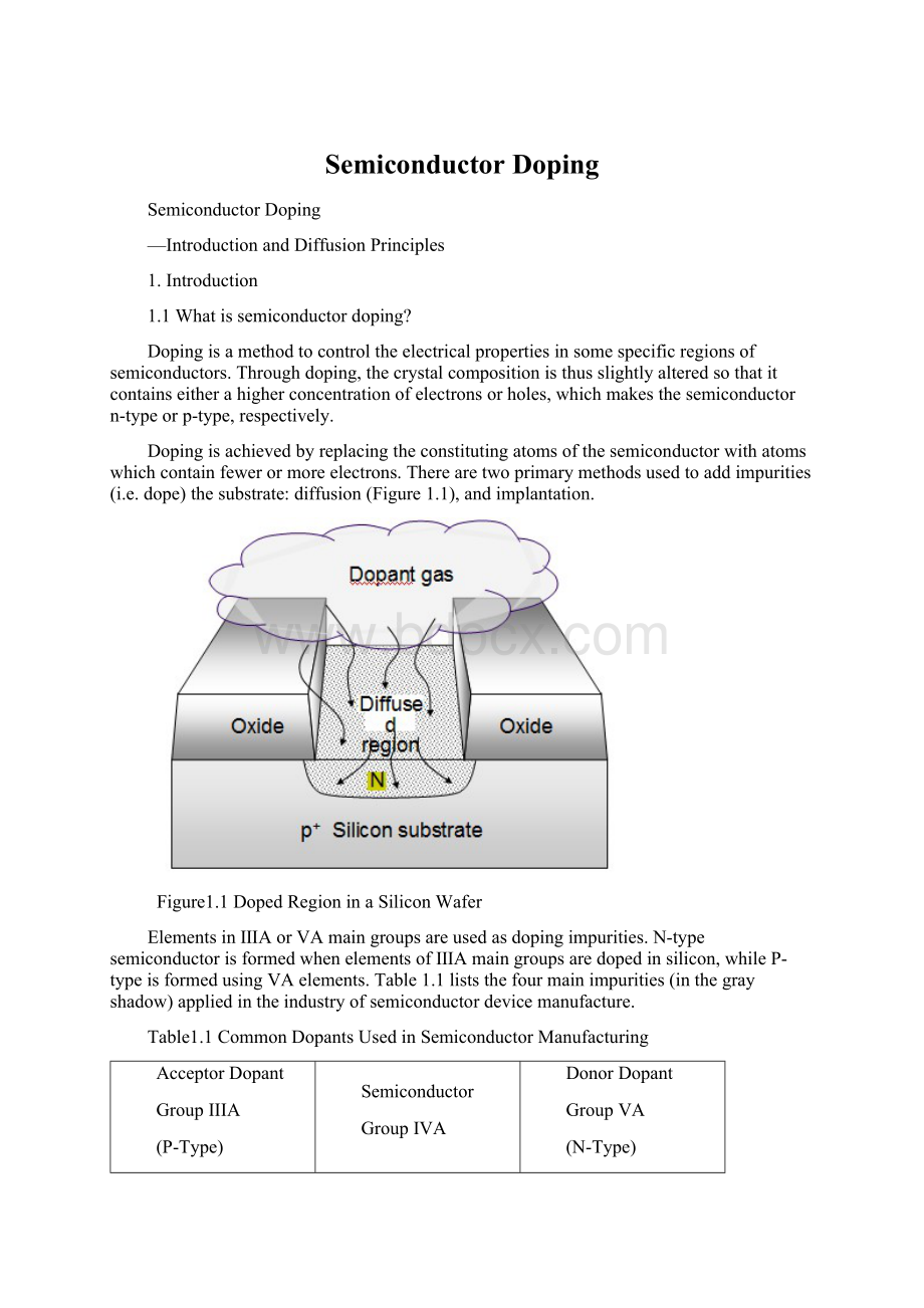
Addingadopingmaterialcanbedoneviadiffusion.Thedopingmaterialfillsemptyspaceswithinthecrystallattice,whileitcomesbetweenthesiliconcompounds.Insomecases,itevenswitchspositionswithsiliconcompounds.Diffusioncanbeachievedviagases(nitrogenandargon)orsolidmaterials,orotherdopingsources.
AsitisshowninFigure1.2(a),amaskinglayer(e.g.PR)isusedtoblockthewafersurfaceexceptwherethedopantsaredesired.Thewaferisplacedinahigh-temperaturefurnace(~1000°
C)wheretheatmospherecontainsthedesiredimpurityingaseousform.Throughtheprocessofdiffusion,impurityatoms,whichareinhighconcentrationintheatmosphere,willdiffuseintothesubstrate,wheretheyhavealowconcentration(initiallyzero).Aftersometime(~0.5–10hours)theimpurityatomsareuniformlydistributedintotheexposedwafersurfaceatashallowdepth(0.5-5mm)ataconcentrationthatcanbereliablycontrolled(~1012-1019cm-3).
1.3.2Ionimplantation
Anotherdopingapproachisionimplantation,whichisveryusefultoalterawaferthathasalreadybeendoped,becauseionimplantationisperformedatambienttemperature.Thispreventsexistingdopantstodiffuse.Itispossibletomaskcertainareasofthewafertotreatonlyveryspecificareas.Thereismuchmoretosayaboutionimplantation,suchasthedepthofpenetration,activationofthedopingadditiveathightemperatures,channeling,diffusingoxidelayers,etc.Thisprocesscanberepeatedmultipletimesduringtheprocess.
Implantationisfunctionallysimilartodiffusion,butheretheatomsare"
shot"
intothewaferathighvelocity(acrossaverystrongelectricfield)andtheyembedthemselvesintothewafersurface(Figure1.2(b)).Ashort(~10min.)annealingstepatelevatedtemperatures(~800°
C)isusedtofitthenewatomsintothesubstratecrystallattice.Implantationismoreuniformacrossthewaferthandiffusionandallowsforveryprecisecontrolofwheretheimpuritieswillbe.Inaddition,itspeakconcentrationcanbebeneaththewafersurface,anditdoesnotrequirealongperiodoftimeathightemperature.However,animplantedjunctionmustremainnearthesurfaceofthewafer(~0.1-2mm)andcannotgoasdeepasadiffusedjunction.Theimpurityconcentrationprofile(concentrationvs.depth)isdifferentfordiffusionandionimplantation,asshowsinFigure1.2.Howeverbotharewellknownandpredictable.
Ionimplantationisveryusefultoalterawaferthathasalreadybeendoped,becauseionimplantationisperformedatambienttemperature.Thispreventsexistingdopantstodiffuse.Itispossibletomaskcertainareasofthewafertotreatonlyveryspecificareas.
Figure1.2Twotypeofdoping:
(a)diffusion;
(b)ionimplanting
1.3DopingprocessofSemiconductorfabricationtechnology
Dopingcanbedoneatthetimethemonocrystalisgrownordonewiththefinalwaferandduringthephotolithographyprocesslateron.Thisallowsforthealterationoftheelectricalpropertiesofspecificareasandspecificlayersinsteadoftheentirecrystalstructure(partialdoping).Mostly,dopingprocessisdoneafterphotolithography.
BasicProcesses:
(1)WaferGrowth:
Creationofsingle-crystalsubstratematerial;
(2)Photolithography:
Definitionofregions(throughamask)onwaferforselectiveprocessing;
(3)Doping:
Additionofdesiredimpuritiesnearthesurfaceofthewafer
(4)Oxidation:
Thermalgrowthofnaturaldielectriclayer(e.g.SiO2)
(5)Deposition:
Additionoflayersofaspecificmaterial(e.g.Si3N4)onthewafersurface
(6)Etching:
Removalofmaterialfromthewafersurface
(7)EpitaxialGrowth:
Reorderingofdepositedmaterialtoformsingle-crystalmaterial
Intheearlytimeofsemiconductordevicemanufacture,diffusionisthemaintoolofdoping.However,asthedecreasingofcharacteristicsizeofsemiconductordevices,ionimplantingisreplacingdiffusinginthemostarea.Figure1.3isthecross-sectiondiagramofaCOMSinverterandthedopingareasareindicated(norpdopingtype,+or–representconcentration).Table1.2showstheparticularprocess(diffusionorionimplantation)ordopantcorrespondstothedopingareainFigure1.3(A~O).AsitisillustratedinTable1.2,ionimplantationmakesupthemajorityofthedopingprocessescomparedtodiffusion.[1]
Figure1.3CMOSStructurewithDopedRegions
Table1.2CommonDopantProcessesinCMOSFabrication
2.Diffusion
2.1CharacteristicofDiffusion
Diffusionisfirstusedtodopesemiconductor,andisgraduallyreplacedbyionimplantationafteritsintroductioninmid-1970s.Nowadays,itisstillwidelyforthedrive-inofdopantandR&
Donultrashallowjunctionformation.Therearesomecharacteristicsofdiffusion:
(1)Isotropicprocess;
(2)Can’tindependentlycontroldopantprofileanddopantconcentration;
(3)Performedinhightemperaturefurnace;
(4)Usingsilicondioxidemask;
(5)Causinglittledamagetothesubstrate.
2.2Diffusionprocess
Mostofthesediffusionprocessesoccurintwosteps:
thepredepositionandthedrive-indiffusion.
2.2.1Predeposition
Inthepredepositionstep,ahighconcentrationofdopantatomsareintroducedatthesiliconsurfacebyavaporthatcontainsthedopantatatemperatureofabout1000°
C(Figure2.1).Atthetemperatureofl000℃,siliconatomsmoveoutoftheirlatticesitescreatingahighdensityofvacanciesandbreakingthebondwiththeneighboringatoms.Theconcentractionofthedopantsnearthesurfaceisaconstant.
Weshouldnotethatpredepositionbydiffusioncanalsobereplacedbyashallowimplantationstep
Figure2.1Predepositionprocessindiffusion
2.2.2Drive-in
Thesecondstepisdriveinprocess,usedtodrivetheimpuritiesdeeperintothesurfacewithoutaddinganymoreimpurities(Figure2.2).Thetotalamountofimpuritiesisaconstant.
Figure2.2thedrive-inprocessindiffusion
Diffusiondepthiscontrolledbythetimeandtemperatureofthedrive-inprocess.Byprecisecontrolofthetimeandtemperature(towithin0.25°
C),accuratejunctiondepthsoffractionofamicroncanbeobtained.
2.2.3Theformationofp-njunction
Thecontrolleddiffusionofdopantsintosilicontoalterthetypeandlevelofconductivityofsemiconductormaterialsisthefoundationofformingap-njunctionandformationofdevicesduringwaferfabrication.
Whendopantofonetype(porn)isdiffusedintoawaferoriginallydopedwithdopantoftheoppositetype,ajunctionwillbeformed,asshowninfigure2.3.Thedistanceofthejunctionfromthesurfaceisknownasthejunctiondepth,xj.Atxjtheconcentrationofthediffuseddopant=theconcentrationofthesubstratedopant(assumedtohaveauniformconcentration),asitisshowninFigure2.3(b).
Itisusedtoformbases,emitters,andresistorsinbipolardevices,aswellasdrainsandsourcesinMOSdevices.Itisalsousedtodopepolysiliconlayers.ItisnotapplicabletoSiCprocessingandotherwidebandgapmaterial.
Figure2.3theformationofp-njunction
2.3Microscopicpointofviewofdopantdiffusion
Thereexistseveraltypesofdiffusionmechanisms.Wetakethediffusionofdopantsinsiliconasanexample.Figure2.4(a)showsaperfectlatticeinsiliconcrystal.Afirstpossiblemechanismconsistsofadopantdirectlydiffusingintoalatticevacancy(Figure2.4(b)).Animpuritycanalsodiffuseintoaninterstitialsiteinthelatticeandcanmovefromtheretoanotherinterstitialsite,asshowninFigure2.4(d).Sometimesasiliconatomcanbeknockedintoaninterstitialsite,leavingavacancyinthelatticewhereadiffusingdopantatomcanfit,whichisnamedasinterstitialdiffusion,asshowninFigure2.4(c).Itisonlyinthecasesthatanimpurityoccupiesavacatedlatticesitethatn-typeorp-typedopingcanoccur.Thepresenceofsuchvacanciesinthelatticecanbeduetodefectsortoheatwhichincreasesatomicvibrationsthusgivingenoughenergytothesiliconatomstomoveoutoftheirequilibriumpositionsintointerstitialsites.Sothediffusionprocessneedshightemperaturesinceweneedtochangetheelectricpropertiesofsemiconductorsthroughdoping.
Figure2.4diffusionmodelsinsilicon
Therearemanydifferenttypesofimpuritiesthatcanbeusedfordiffusion,themost


- 配套讲稿:
如PPT文件的首页显示word图标,表示该PPT已包含配套word讲稿。双击word图标可打开word文档。
- 特殊限制:
部分文档作品中含有的国旗、国徽等图片,仅作为作品整体效果示例展示,禁止商用。设计者仅对作品中独创性部分享有著作权。
- 关 键 词:
- Semiconductor Doping
 冰豆网所有资源均是用户自行上传分享,仅供网友学习交流,未经上传用户书面授权,请勿作他用。
 对中国城市家庭的教育投资行为的理论和实证研究.docx
-
二年级下册数学练习题大全.docx
-
二十年后回故乡的优秀作文.docx
-
软基换填施工方案.docx
-
《黑白装饰画》教案.docx
-
课堂教学改革实施方案5篇.docx
-
返璞归真简约致美解读《给予树》教学设计语文.docx
-
离职证明范本精选多篇.docx
-
《天局》全文.docx
-
我害怕作文集合15篇.docx
-
伏魔战记39详细攻略.docx
-
幼儿园学期计划.docx
-
雅思分类打印版Word格式文档下载.docx
-
年产1万吨竹子纤维加工项目可行性研究报告文档格式.docx
-
电商产业化项目投资经营商业计划书Word文件下载.docx
-
医学多媒体课件的设计与制作Word文档格式.docx
-
中学生中秋节想象作文Word格式.docx
-
等保20之漏洞扫描系统技术方案建议书Word文档格式.docx
-
培训学校个人工作计划模板5篇Word格式.docx
-
北京各区二模试题分类汇编文言文阅读Word文档下载推荐.docx
-
不同职业病危害因素的防护常识Word格式文档下载.docx
-
一年级上册同音形近字练习汇总Word文档格式.docx
-
班级家长会上班主任教师讲话稿Word下载.docx
-
科斯塔环载波恢复Word文件下载.docx
-
浙教义务版六年级语文下册教案 花潮Word文件下载.docx
-
集成电路设计与集成系统专业Word格式文档下载.docx
-
开工第一课专题讲座观后感文档格式.docx
-
东城区学年第一学期高三期末化学试题及答案Word格式文档下载.docx
-
苏教版六年级语文下册第七单元测试题Word格式文档下载.docx
-
学长征精神做红色传人活动方案文档格式.docx
-
读书笔记150字30篇文档格式.docx
-
中级经济法考前必背法条精华版备考资料Word格式.docx
-
浙江省地方水利建设基金征收和减免管理办法.docx
-
浙江省中医药继续教育项目.docx
-
整理产业集群发展工作意见.docx
-
执业医师题目汇总2教案.docx
-
职教第二册第二单元教案.docx
-
制度晋煤生产制度汇编.docx
-
中国传统文化概观模拟试题1.docx
-
中国矿业大学语文大纲.docx
-
中级会计师职称试题及答案.docx
-
中级经济师考试经济基础知识常考题型.docx
-
香格蔚蓝工程施工组织设计二期.docx
-
湘潭至湘乡二公路改建工程概况.docx
-
项目管理的约束条件.docx
-
项目经理述职报告.docx
-
橡胶类零部件标准.docx
-
消防应急演练资料.docx
-
小班认识610的教案.docx
-
小口径单座调节阀KHLS小口径单座调节阀.docx
-
小升初第13讲 计数的方法与原理.docx
